KLA forecasts mid-to-high teens percentage growth for its advanced packaging business in calendar 2026, driven by AI accelerator production requirements. The projection indicates packaging equipment sales are accelerating faster than front-end semiconductor manufacturing tools.
AI chips like GPUs and custom accelerators increasingly use 2.5D and 3D packaging to stack memory dies next to compute chiplets. This architecture reduces latency and power consumption compared to traditional PCB layouts. Companies building these systems need specialized inspection and metrology equipment—KLA's core business.
Lumentum posted over 65% year-over-year revenue growth in its latest quarter, with management expecting to exceed $750 million in quarterly revenue next quarter. The company supplies optical components and interconnects used in advanced packaging applications.
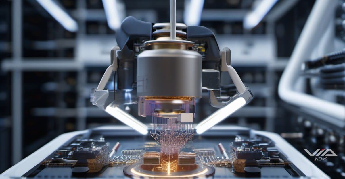
The packaging shift addresses physical limits in chip scaling. As transistor shrinking slows, chipmakers gain performance by placing multiple dies closer together using through-silicon vias and interposers. Each AI accelerator module now contains multiple dies requiring precision alignment measured in microns.
Traditional packaging wrapped individual chips in plastic. Advanced packaging builds multi-die systems before final encapsulation. This requires new process steps: wafer thinning, micro-bump deposition, hybrid bonding. Each step needs inspection equipment to maintain yields.
KLA's performance exceeds broader industry trends, suggesting it holds strong positions in critical packaging process steps. The company provides defect inspection for wafer-level packaging and metrology tools that measure bump heights and alignment accuracy.
The packaging equipment market historically represented 10-15% of total semiconductor capital spending. If KLA's forecast holds and peers see similar growth, that ratio will climb. Equipment suppliers with packaging exposure may outperform those focused solely on traditional lithography and etching.
This growth pattern differs from previous chip booms. In past cycles, front-end equipment—lithography, deposition, etching—drove capital spending. Now packaging tools are taking a larger share as chip architecture evolves from monolithic dies to heterogeneous multi-chip modules.